Take part in the Briefing for FYP 2 students held at TTL 1 on Wednesday at 3pm.
Get to know the procedures how to claim, hw to prepare for FYP 2
for more information visit (http://fyp.bmi.unikl.edu. my/index.php) (UNIKL BMI website).
Wednesday, October 28, 2015
Thursday, October 22, 2015
Fyp 2: Week 8 :- Final Year Project 2
Relay Switch Circuit
The Relay Switch Circuit
Relays are electromechanical devices that use an electromagnet to operate a pair of movable contacts from an open position to a closed position. The advantage of relays is that it takes a relatively small amount of power to operate the relay coil, but the relay itself can be used to control motors, heaters, lamps or AC circuits which themselves can draw a lot more electrical power.
The Electro-mechanical Relay is an output device (actuator) which come in a whole host of shapes, sizes and designs, and have many uses and applications in electronic circuits. But while electrical relays can be used to allow low power electronic or computer type circuits to switch relatively high currents or voltages both “ON” or “OFF”, some form of relay switch circuit is required to control it.
The design and types of relay switching circuits is huge, but many small electronic projects use transistors and MOSFETs as their main switching device as the transistor can provide fast DC switching (ON-OFF) control of the relay coil from a variety of input sources so here is a small collection of some of the more common ways of switching relays.
NPN Relay Switch Circuit
A typical relay switch circuit has the coil driven by a NPN transistor switch, TR1 as shown depending on the input voltage level. When the Base voltage of the transistor is zero (or negative), the transistor is cut-off and acts as an open switch. In this condition no Collector current flows and the relay coil is de-energised because being current devices, if no current flows into the Base, then no current will flow through the relay coil.
If a large enough positive current is now driven into the Base to saturate the NPN transistor, the current flowing from Base to Emitter (B to E) controls the larger relay coil current flowing through the transistor from the Collector to Emitter.
For most bipolar switching transistors, the amount of relay coil current flowing into the Collector would be somewhere between 50 to 800 times that of the required Base current to drive the transistor into saturation. The current gain, or beta value ( β ) of the general purpose BC109 shown is typically about 290 at 2mA (Datasheet).
NPN Relay Switch Circuit

Note that the relay coil is not only an electromagnet but it is also an inductor. When power is applied to the coil due to the switching action of the transistor, a maximum current will flow as a result of the DC resistance of the coil as defined by Ohms Law, (I = V/R). Some of this electrical energy is stored within the relay coil’s magnetic field.
When the transistor switches “OFF”, the current flowing through the relay coil decreases and the magnetic field collapses. However the stored energy within the magnetic field has to go some where and a reverse voltage is developed across the coil as it tries to maintain the current in the relay coil. This action produces a high voltage spike across the relays coil that can damage the switching NPN transistor if allowed to build up.
So in order to prevent damage to the semiconductor transistor, a “flywheel diode”, also known as a freewheeling diode, is connected across the relay coil. This flywheel diode clamps the reverse voltage across the coil to about 0.7V dissipating the stored energy and protecting the switching transistor. Flywheel diodes are only applicable when the supply is a polarized DC voltage. An AC coil requires a different protection method, and for this an RC snubber circuit is used.
NPN Darlington Relay Switch Circuit
The previous NPN transistor relay switch circuit is ideal for switching small loads such as LED’s and miniature relays. But sometimes it is required to switch larger relay coils or currents beyond the range of a BC109 general purpose transistor and this can be achieved using Darlington Transistors.
The sensitivity and current gain of a relay switch circuit can be greatly increased by using a Darlington pair of transistors in place of a single switching transistor. Darlington Transistor pairs can be made from two individually connected Bipolar Transistors as shown or available as one single device with standard: Base, Emitter and Collector connecting leads.
The two NPN transistors are connected as shown so that the Collector current of the first transistor,TR1 becomes the Base current of the second transistor TR2. The application of a positive base current to TR1 automatically turns “ON” the switching transistor, TR2.
NPN Darlington Relay Switch Circuit

If two individual transistors are configured as a Darlington switching pair, then a small value resistor (100 to 1,000Ω’s) is usually placed between the Base and Emitter of the main switching transistor, TR2 to ensure that it turns fully OFF. Again a flywheel diode is used to protect TR2 from the back emf generated when the relay coil is de-energised.
Emitter Follower Relay Switch Circuit
As well as the standard Common Emitter configuration for a relay switch circuit, the relay coil can also be connected to the Emitter terminal of the transistor to form an Emitter Follower circuit. The input signal is connected directly to the Base, while the output is taken from the Emitter load as shown.
Emitter Follower Relay Switch Circuit

The Common Collector, or Emitter Follower configuration is very useful for impedance matching applications because of the very high input impedance, in the region of hundreds of thousands of Ohms while having a relatively low output impedance to switch the relays coil. As with the previous NPN relay switch circuit, switching occurs by applying a positive current to the base of the transistor.
Emitter Darlington Relay Switch Circuit
This is the Darlington transistor version of the previous Emitter Follower circuit. A very small positive Base current applied to TR1 causes a much greater Collector current to flow through TR2due to the multiplication of the two Beta values.
Emitter Darlington Relay Switch Circuit

The Common Emitter Darlington relay switch circuit is useful to provide current gain and power gain with the voltage gain approximately equal to unity. Another important characteristic of this type of Emitter Follower circuit is that it has a high input impedance and a low output impedance, which make it ideal for impedance matching to large relay coils.
PNP Relay Switch Circuit
As well as switching relay coils and other such loads with NPN Bipolar Transistors, we can also switch them using PNP Bipolar Transistors. The PNP relay switch circuit is no different to the NPN relay switching circuit in terms of its ability to control the relays coil. However, it does require different polarities of operating voltages. For example, the Collector-Emitter voltage, Vce , must be negative for the PNP type to cause current flow from the Emitter to the Collector.
PNP Relay Switch Circuit

The PNP transistor circuit works in opposite to the NPN relay switching circuit. Load current flows from the Emitter to the Collector when the Base is forward biased with a voltage that is more negative than that at the Emitter. For the relays load current to flow through the Emitter to the Collector, both the Base and the Collector must be negative in respect to the Emitter.
In other words, when Vin is HIGH the PNP transistor is switched “OFF” and so too is the relay coil. When Vin is LOW, the Base voltage is less than the Emitter voltage, (more negative) and the PNP transistor turns “ON”. The Base resistor value sets the Base current, which sets the Collector current that drives the relay coil.
PNP transistor switches can be used when the switching signal is the reverse for an NPN transistor, for example the output of a CMOS NAND gate or other such logic device. A CMOS logic output has the drive strength at logic 0 to sink sufficient current to turn the PNP transistor “ON”. Then current sinks can be turned into current sources by using PNP transistors and a power supply of opposite polarity.
PNP Collector Relay Switch Circuit
The operation of this circuit is the same as the previous relay switching circuit. In this relay switch circuit, the relay load has been connected to the PNP transistors Collector. The ON-OFF switching action of the transistor and coil occurs when Vin is LOW, transistor “ON” and when Vin is HIGH, transistor “OFF”.
PNP Collector Relay Switch Circuit

We have seen that either an NPN bipolar transistor or an PNP bipolar transistor can operate as a switch for relay switching, or any other load for that matter. But that there are two different conditions that need to be understood as the current flows in two different directions.
So in an NPN transistor, a HIGH voltage with respect to the Emitter is applied to the Base, current flows from the Collector to the Emitter and the NPN transistor switches “ON”. For a PNP transistor, a LOW voltage with respect to the Emitter is applied to the Base, current flows from the Emitter to the Collector and the PNP transistor switches “ON”.
N-channel MOSFET Relay Switch Circuit
MOSFET relay switching operation is very similar to Bipolar Junction Transistor (BJT) switch operation seen above, and any of the previous circuits can be implemented using MOSFETs. However, there are some major differences in the operation of the MOSFET circuits with the main ones being that MOSFETs are voltage operated devices, and as the Gate is electrically isolated from the Drain-Source channel, they have very high input impedances so the Gate current for a MOSFET is zero, therefore a base resistor is unnecessary.
MOSFETs conduct through a conductive channel with the channel initially being closed, transistor “OFF”. This channel gradually increasing in conductive width as the voltage applied to the Gate terminal is slowly increased. In other words, the transistor operates by enhancing the channel as the Gate voltage increases and for this reason the this type of MOSFET is called an Enhancement MOSFET, or E-MOSFET.
N-channel Enhancement MOSFETs (NMOS) are the most commonly used type of MOSFET as a positive voltage on the Gate terminal switches the MOSFET “ON” and zero or a negative voltage on the Gate switches it “OFF”, making ideal as MOSFET relay switch. Complementary P-channel Enhancement MOSFETs are also available which, like the PNP BJT work with opposite voltages.
N-channel MOSFET Relay Switch Circuit

The above MOSFET relay switch circuit is connected in a common-source configuration. With zero voltage input, LOW condition, the value of VGS, there is insufficient Gate drive to open the channel and the transistor is “OFF”. But when VGS is increased above the MOSFETs lower threshold voltageVT, the channel opens, current flows and the relay coil is operated.
Then the enhancement mode MOSFET operates as a normally open switch making it ideal for switching small loads such as relays. E-type MOSFETs have high “OFF” resistance but moderate “ON” resistance (OK for most applications), so when selecting one for a particular switching application, its RDS value needs to be taken into consideration.
P-channel MOSFET Relay Switch Circuit
The P-channel Enhancement MOSFET (PMOS) is constructed the same as for the N-channel Enhancement MOSFET except that it operates with negative Gate voltages only. In other words, A P-channel MOSFET operates in the same fashion but with opposite polarities as the Gate must be more negative than the Source to turn “ON” the transistor by being forward-biased as shown.
P-channel MOSFET Relay Switch Circuit

In this configuration, the P-channels Source terminal is connected to +Vdd and the Drain terminal is connected to ground via the relays coil. When a HIGH voltage level is applied to the Gate, the P-channel MOSFET will be turned “OFF”. The turned “OFF” E-MOSFET will have a very high channel resistance and acts nearly like an open circuit.
When a LOW voltage level is applied to the Gate, the P-channel MOSFET will be turned “ON”. This will cause current to flow through the low resistance path of e-MOSFETs channel operating the relay coil. Both N-channel and P-channel e-MOSFETs make excellent low voltage relay switching circuits and can easily be interfaced to a wide variety of digital logic gates and micro-processor applications.
Logic Controlled Relay Switch Circuit
The N-channel, enhancement-type MOSFET is extremely useful as a transistor switch because in its “OFF” state (with zero Gate bias) its channel has a very high resistance blocking current flow. However, a relatively small positive voltage greater than the threshold voltage VT, on its high impedance Gate causes it to begin conducting current from its Drain terminal to its Source terminal.
Unlike the Bipolar Junction Transistor which requires a Base current to turn it “ON”, the e-MOSFET only requires a voltage on the Gate as due to its insulated Gate construction, zero current flows into the Gate. Then this makes the e-MOSFET, either N-channel or P-channel ideal to be driven directly by typical TTL or CMOS logic gates as shown.
Logic Controlled Relay Switch Circuit

Here the N-channel E-MOSFET is being driven by a digital logic gate. The output pins of most logic gates can only supply a limited amount of current, typically no more than about 20 mA. As e-MOSFETs are voltage operated devices and consume no Gate current, we can use a MOSFET relay switch circuit to control high power loads.
Micro-controller Relay Switch Circuit
As well as digital logic gates, we can also use the output pins and channels of micro-controllers, PIC’s and processors to control the outside world. The circuit below shows how to interface a relay using a MOSFET switch.
Micro-controller Relay Switch Circuit

Relay Switching Circuit Summary
In this tutorial we have seen how we can use both Bipolar Junction Transistors, either NPN or PNP and Enhancement MOSFETs, either N-channel or P-channel as a transistor switching circuit.
Sometimes when building Electronic or Micro-controller circuits we want to use a transistor switch to control a high-power device, such as motors, lamps, heating elements or AC circuits. Generally these devices require larger currents or higher voltages than a single power transistor can handle then we can use a relay switching circuit to do this.
Bipolar transistors (BJT’s) make very good and cheap relay switching circuits, but BJT’s are current operated devices as they convert a small Base current into a larger load current to energise the relay coil.
However, the MOSFET switch is ideal as an electrical switch as it takes virtually no Gate current to turn “ON”, converting a Gate voltage into a load current. Therefore, a MOSFET can be operated as a voltage-controlled switch.
In many applications bipolar transistors can be substituted with enhancement-type MOSFETs offering faster switching action, much higher input impedance, and probably less power dissipation. The combination of a very high Gate impedance, very low power consumption in its “OFF” state, and very fast switching capability makes the MOSFET suitable for many digital switching applications. Also with zero Gate current its switching action can not overload the output circuit of a digital gate or micro-controller.
However, because the gate of an E-MOSFET is insulated from the rest of the component, it is especially sensitive to static electricity which could destroy the thin oxide layer on the Gate. Then special care should be taken either when handling the component, or when it is in use and that any circuit using e-MOSFETs includes appropriate protection from static and voltage spikes.
Also for additional protection of either BJT’s or MOSFETs, always use a flywheel diode across and relay coil to safely dissipate the back emf generated by the transistors switching action.
Thursday, October 15, 2015
Fyp 2: Week 7 :- Final Year Project 2
Take part in the Briefing for FYP 2 students held at TTL 1 on Wednesday at 3pm.
Get to know the procedures involve in completing FYP 2 at (http://fyp.bmi.unikl.edu. my/index.php) (UNIKL BMI website).
FYP Briefing #2
- Project
Development
- Methodology used
- Results analysis
- Report writing
- Accomplishment
and major findings
Get to know the procedures involve in completing FYP 2 at (http://fyp.bmi.unikl.edu. my/index.php) (UNIKL BMI website).
- Project
Development
- Methodology used
- Results analysis
- Report writing
- Accomplishment
and major findings
Saturday, October 10, 2015
Fyp 2: Week 6 :- Final Year Project 2
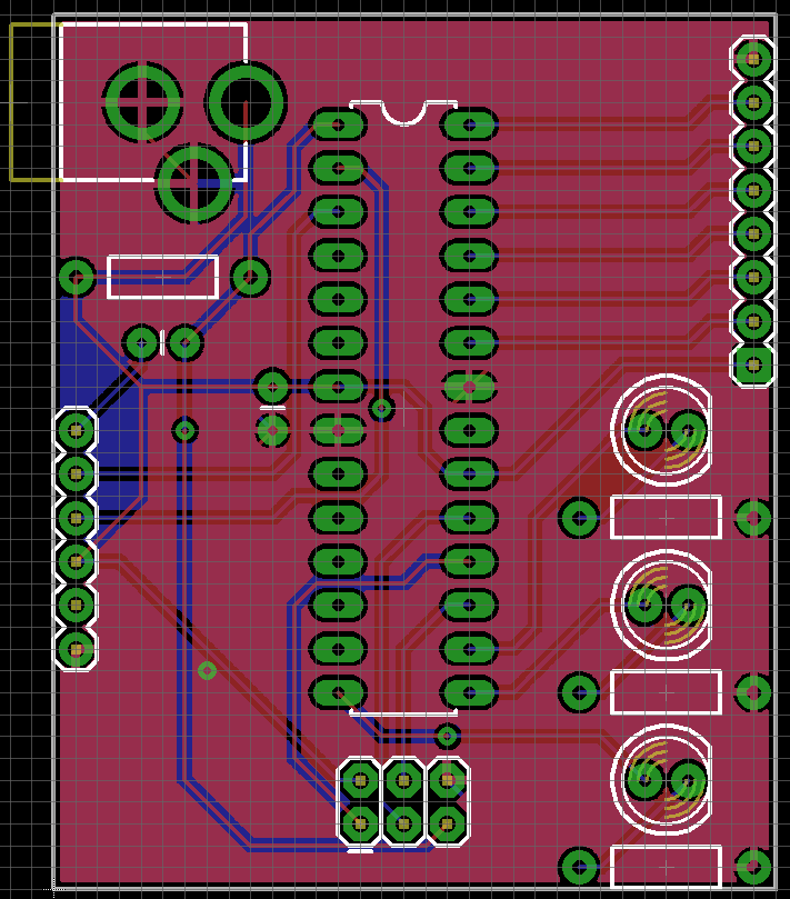
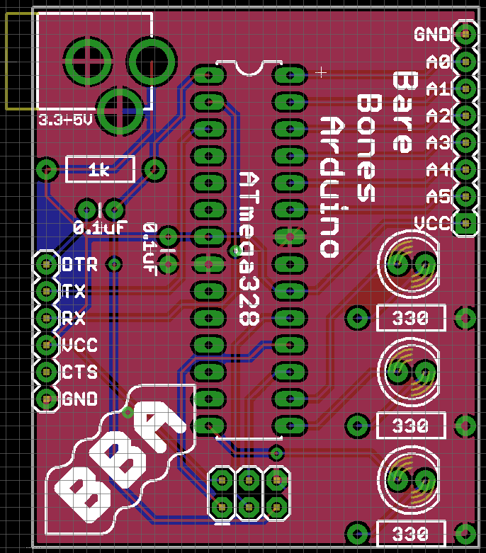
Using EAGLE: Board Layout
Step EAGLE PCB design: from placing parts, to routing them, to generating gerber files to send to a fab house. The basics of EAGLE’s board editor, beginning with explaining how the layers in EAGLE match up to the layers of a PCB.
Create a Board From Schematic
Before starting this tutorial, read through and follow along with the Using EAGLE: Schematic tutorial (not to mention the Setting Up EAGLE tutorial before that). The schematic designed in that tutorial will be used as the foundation for the PCB designed here.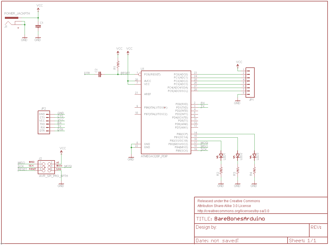
The schematic from previous tutorial,
complete with an ATmega328P, barrel jack connector, LEDs, resistors,
capacitors, and connectors.
 (on the top toolbar, or under the File
menu) – which should prompt a new, board editor window to open. All of
the parts you added from the schematic should be there, stacked on top
of eachother, ready to be placed and routed.
(on the top toolbar, or under the File
menu) – which should prompt a new, board editor window to open. All of
the parts you added from the schematic should be there, stacked on top
of eachother, ready to be placed and routed.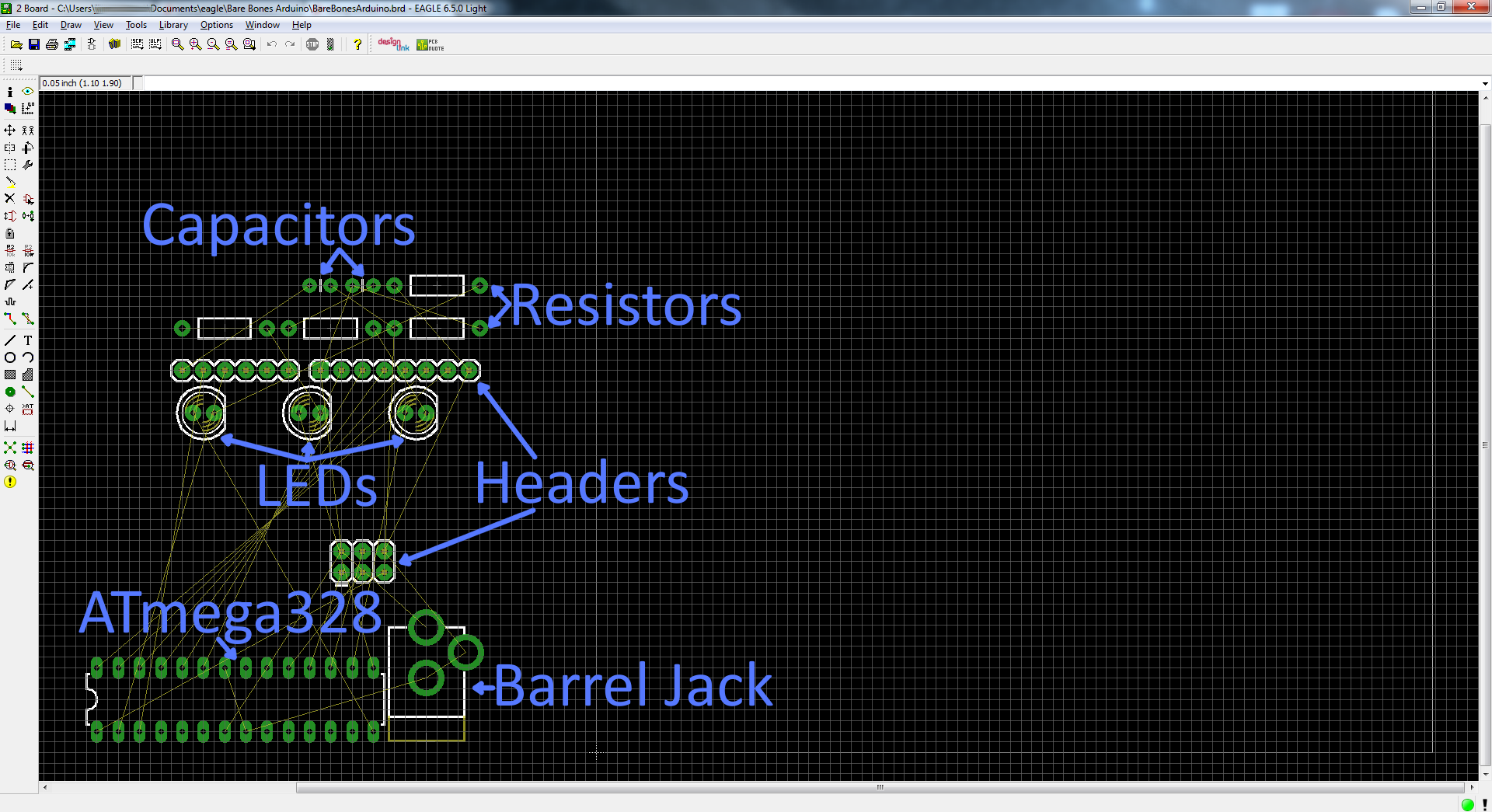
Layers Overview
PCB composition is all about layering one material over another. The thickest, middle part of the board is a insulating substrate (usually FR4). On either side of that is a thin layer of copper, where our electric signals pass through. To insulate and protect the copper layers, we cover them with a thin layer of lacquer-like soldermask, which is what gives the PCB color (green, red, blue, etc.). Finally, to top it all off, we add a layer of ink-like silkscreen, which can add text and logos to the PCB.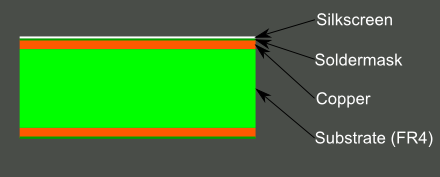
The layers of a double-sided PCB (image from the PCB Basics tutorial).
EAGLE’s Layers
The EAGLE board designer has layers just like an actual PCB, and they overlap too. We use a palette of colors to represent the different layers. Here are the layers you’ll be working with in the board designer:| Color | Layer Name | Layer Number | Layer Purpose |
|---|---|---|---|
| Top | 1 | Top layer of copper | |
| Bottom | 16 | Bottom layer of copper | |
| Pads | 17 | Through-hole pads. Any part of the green circle is exposed copper on both top and bottom sides of the board. | |
| Vias | 18 | Vias. Smaller copper-filled drill holes used to route a signal from top to bottom side. These are usually covered over by soldermask. Also indicates copper on both layers. | |
| Unrouted | 19 | Airwires. Rubber-band-like lines that show which pads need to be connected. | |
| Dimension | 20 | Outline of the board. | |
| tPlace | 21 | Silkscreen printed on the top side of the board. | |
| bPlace | 22 | Silkscreen printed on the bottom side of the board. | |
| tOrigins | 23 | Top origins, which you click to move and manipulate an individual part. | |
| bOrigins | 24 | Origins for parts on the bottom side of the board. | |
| / / Hatch | tStop | 29 | Top stopmask. These define where soldermask should not be applied. |
| \ \ Hatch | bStop | 30 | Absent soldermask on the bottom side of the board. |
| Holes | 45 | Non-conducting (not a via or pad) holes. These are usually drill holes for stand-offs or for special part requirements. | |
| tDocu | 51 | Top documentation layer. Just for reference. This might show the outline of a part, or other useful information. |
To turn any layer off or on, click the “Layer Settings…” button –
 – and then click a layer’s number to select or de-select it. Before you
start routing, make sure the layers above (aside from tStop and bStop)
are visible.
– and then click a layer’s number to select or de-select it. Before you
start routing, make sure the layers above (aside from tStop and bStop)
are visible.Selecting From Overlapping Objects
Here’s one last tip before we get to laying our board out. This is an interface trick that trips a lot of people up. Since the board view is entirely two-dimensional, and different layers are bound to overlap, sometimes you have to do some finagling to select an object when there are others on top of it.Normally, you use the mouse’s left-click to select an object (whether it’s a trace, via, part, etc.), but when there are two parts overlapping exactly where you’re clicking, EAGLE doesn’t know which one you want to pick up. In cases like that, EAGLE will pick one of the two overlapping objects, and ask if that’s the one you want. If it is, you have to left-click again to confirm. If you were trying to grab one of the other overlapping objects, right-click to cycle to the next part. EAGLE’s status box, in the very bottom-left of the window, provides some helpful information when you’re trying to select a part.
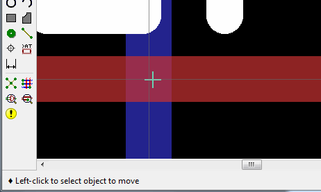
For example: In the GIF above, a VCC net overlaps another named Reset. We left-click once directly where they overlap, and EAGLE asks us if we meant to select VCC. We right-click to cycle, and it asks us instead if we’d like to select Reset. Right-clicking again cycles back to VCC, and a final left-click selects that as the net we want to move.
Arranging the Board
Create a Board From Schematic
If you haven’t already, click the Generate/Switch to Board icon – – in the schematic editor to create a new PCB design based on your schematic: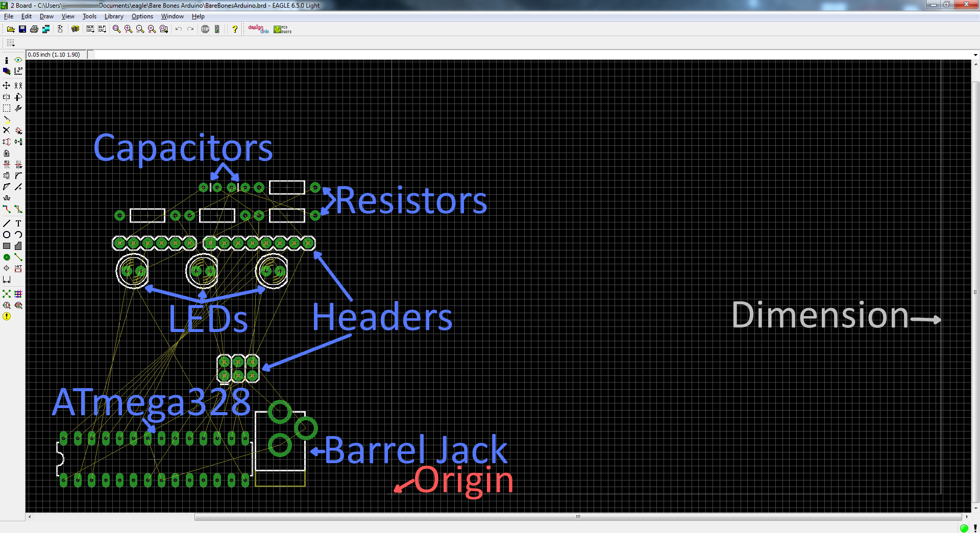
The new board file should show all of the parts from your schematic. The gold lines, called airwires, connect between pins and reflect the net connections you made on the schematic. There should also be a faint, light-gray outline of a board dimension to the right of all of the parts.
Our first job in this PCB layout will be arranging the parts, and then minimizing the area of our PCB dimension outline. PCB costs are usually related to the board size, so a smaller board is a cheaper board.
Understanding the Grid
In the schematic editor we never even looked at the grid, but in the board editor it becomes much more important. The grid should be visible in the board editor. You can adjust the granularity of the grid, by clicking on the GRID icon – . A 0.05" grid, and 0.005" alternate grid is a good size for this kind of board.
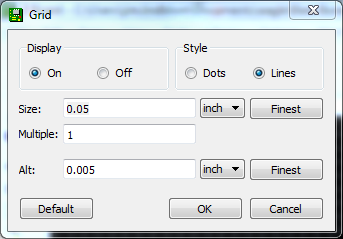
Moving Parts
Using the MOVE tool – – you can start to move parts within the dimension box. While you’re moving parts, you can rotate them by either right-clicking or changing the angle in the drop-down box near the top.
The way you arrange your parts has a huge impact on how easy or hard the next step will be. As you’re moving, rotating, and placing parts, there are some factors you should take into consideration:
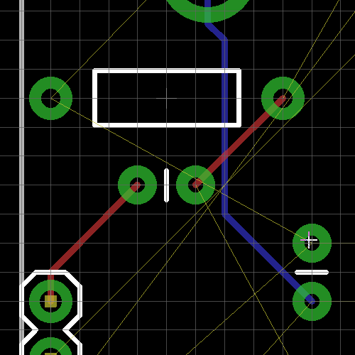
- Don’t overlap parts: All of your components need some space to breathe. The green via holes need a good amount of clearance between them too. Remember those green rings are exposed copper on both sides of the board, if copper overlaps, streams will cross and short circuits will happen.
- Minimize intersecting airwires: While you move
parts, notice how the airwires move with them. Limiting criss-crossing
airwires as much as you can will make routing much easier in the long run. While you’re relocating parts, hit the RATSNEST button –
 – to get the airwires to recalculate.
 - Part placement requirements: Some parts may require special consideration during placement. For example, you’ll probably want the insertion point of the barrel jack connector to be facing the edge of the board. And make sure that decoupling capacitor is nice and close to the IC.
- Tighter placement means a smaller and cheaper board, but it also makes routing harder.
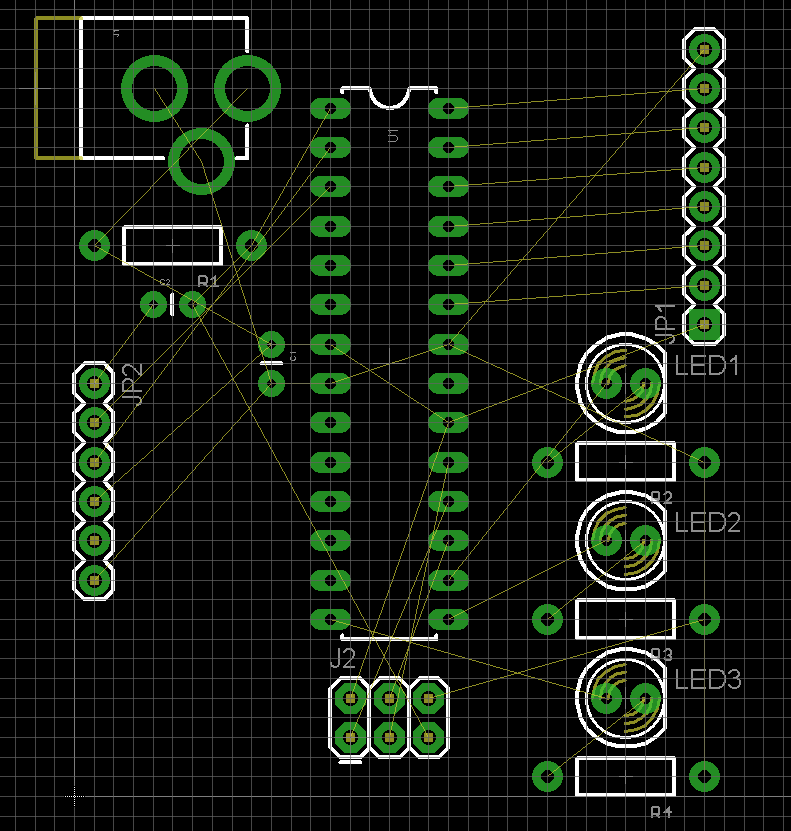
Note: The tNames layer (which isn’t visible by default) was turned on to help identify which part is which.
Adjusting the Dimension Layer
Now that the parts are placed, we’re starting to get a better idea of how the board will look. Now we just need to fix our dimension outline. You can either move the dimensions lines that are already there, or just start from scratch. Use the DELETE tool – – to erase all four of the dimension lines.
Then use the WIRE tool – (
 – to draw a new outline. Before you draw anything though, go up to the options bar and set the layer to 20 Dimension. Also up there, you may want to turn down the width a bit (we usually set it to 0.008").
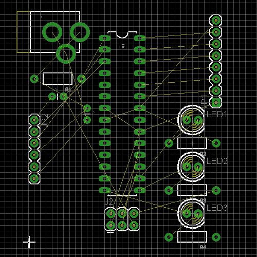
That’s a fine start. With the parts laid out, and the dimension adjusted, we’re ready to start routing some copper!
Routing the Board
Routing is the most fun part of this entire process. It’s like solving a puzzle! Our job will be turning each of those gold airwires into top or bottom copper traces. At the same time, you also have to make sure not to overlap two different signals.Using the Route Tool
To draw all of our copper traces, we’ll use the ROUTE tool– – (not the WIRE tool!). After selecting the tool, there are a few options to consider on the toolbar above:
- Layer: On a 2-layer board like this, you’ll have to choose whether you want to start routing on the top (1) or bottom (16) layer.
- Bend Style: Usually you’ll want to use 45° angles for your routes (wire bend styles 1 and 3), but it can be fun to make loopy traces too.
- Width: This defines how wide your copper will be. Usually 0.01" is a good default size. You shouldn’t go any smaller than 0.007" (or you’ll probably end up paying extra). Wider traces can allow for more current to safely pass through. If you need to supply 1A through a trace, it’d need to be much wider (to find out how much, exactly, use a trace width calculator).
- Via Options: You can also set a few via characteristics here. The shape, diameter, and drill can be set, but usually the defaults (round, auto, and 0.02" respectively) are perfect.
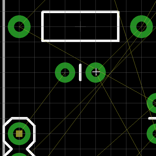
While routing it’s important to avoid two cases of overlap: copper over vias, and copper over copper. Remember that all of these copper traces are basically bare wire. If two signals overlap, they’ll short out, and neither will do what it’s supposed to.
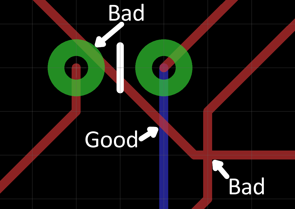
If traces do cross each other, make sure they do so on opposite sides of the board. It’s perfectly acceptable for a trace on the top side to intersect with one on the bottom. That’s why there are two layers.
If you need more precise control over your routes, you can hold down the ALT key on your keyboard to access the alternate grid. By default, this is set to be a much more fine 0.005".
Placing Vias
Vias are really tiny drill holes that are filled with copper. We use them mid-route to move a trace from one side of the board to the other.To place a via mid-route, first left-click in the black ether between pins to “glue” your trace down. Then you can either change the layer manually in the options bar up top, or click your middle mouse button to swap sides. And continue routing to your destination. EAGLE will automatically add a via for you.
Route Clearance
Make sure you leave enough space between two different signal traces. PCB fabricators should have clearly defied minimum widths that they’ll allow between traces – probably around 0.006" for standard boards. As a good rule-of-thumb, if you don’t have enough space between two traces to fit another (not saying you should), they’re too close together.Ripping Up Traces
Much like the WIRE tool isn’t actually used to make wires, the DELETE tool can’t actually be used to delete traces. If you need to go back and re-work a route, use the RIPUP tool – – to remove traces. This tool turns routed traces back into airwires.
You can also use UNDO and REDO to back/forward-track.
Route Away!
That’s about all the simple rules there are. Go have the time of your life solving the routing puzzle! You may want to start on the closest, easiest traces first. Or, you might want to route the important signals – like power and ground – first. Here’s an example of a fully-routed board: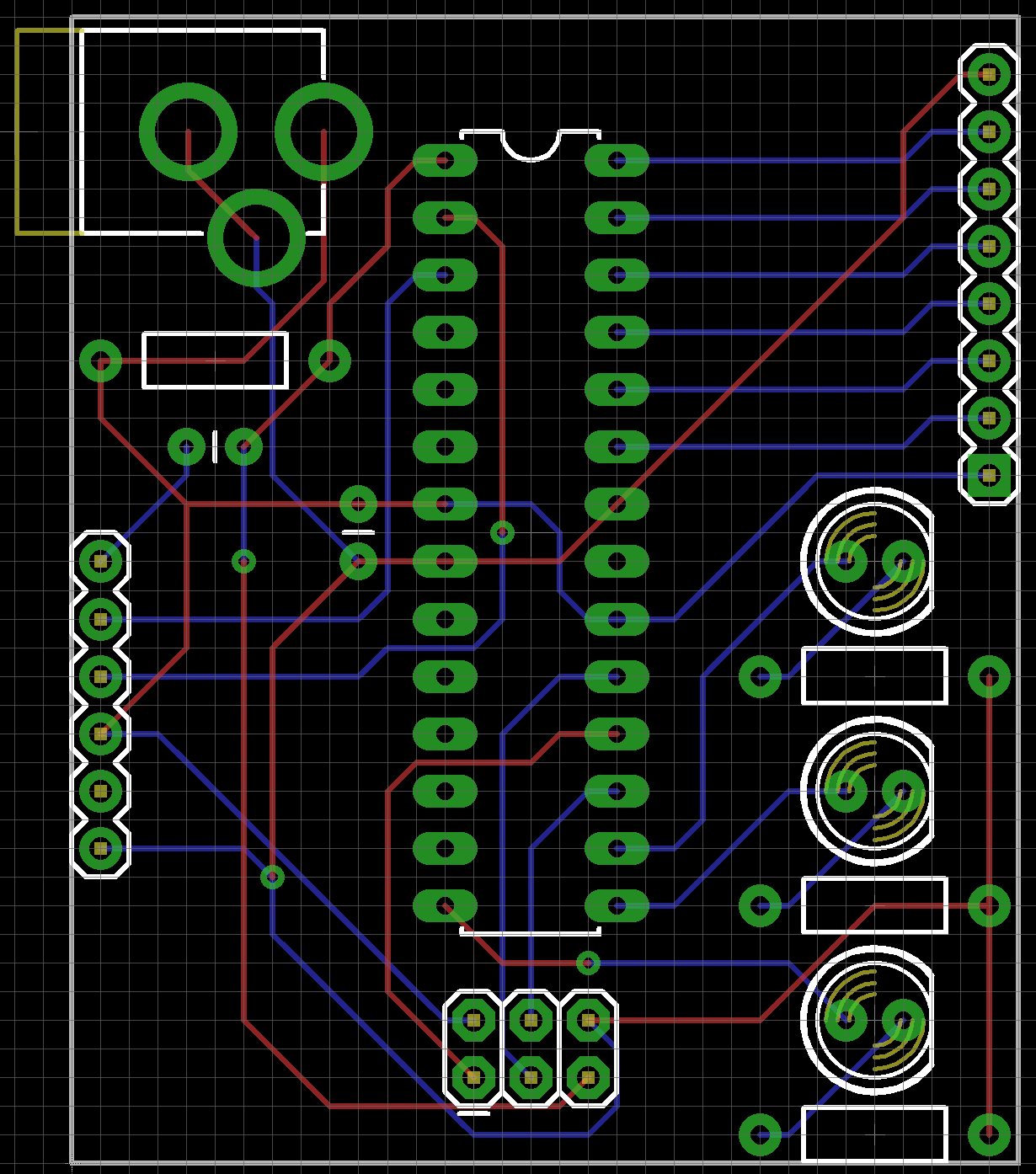
See if you can do a better job than that! Make your board smaller. Or try to avoid using any vias.
After you feel like the routing is done, there are a few checks we can do to make sure it’s 100% complete. We’ll cover those on the next page.
Or Use the Autorouter (Cheater!)
If you’re short on time, or having trouble solving the routing puzzle, you can try loading up EAGLE’s Autorouter – – to see if it can finish the job. Open up the autorouter, don’t worry about these other tabs for now, just click OK.
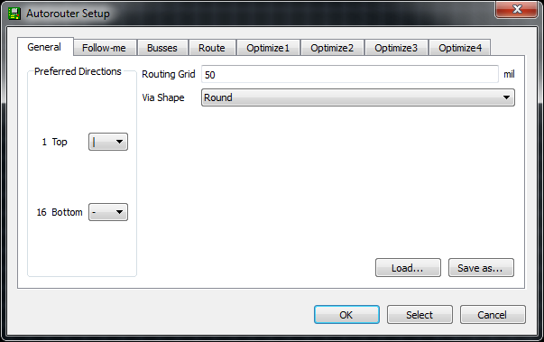
If you don’t like the job the autorouter did, you can quickly hit Undo to go back to where you were.
The autorouter won’t always be able to finish the job, so it’s still important to understand how to manually route pads (plus manual routes look much better). After running the autorouter, check the bottom-left status box to see how it did. If it says anything other than “OptimizeN: 100% finished”, you’ve still got some work to do. If your autorouter couldn’t finish the job, try turning Routing Grid down from 50mil 10mil.
There are tons of optimizations and settings to be made in the autorouter. If you want to dig deeper into the subject, consider checking out EAGLE’s manual where an entire chapter is devoted to it.
Checking for Errors
Before we package the design up and send it off to the fabrication house, there are a few tools we can use to check our design for errors.Ratsnest – Nothing To Do!
The first check is to make sure you’ve actually routed all of the nets in your schematic. To do this, hit the RATSNEST icon – – and then immediately check the bottom left status box. If you’ve routed everything, it should say “Ratsnest: Nothing to do!”
If ratsnest says you have “N airwires” left to route, double check your board for any floating golden lines and route them up. If you’ve looked all over, and can’t find the suspect airwire, try turning off every layer except 19 Unrouted.
Design Rule Check
Once you’re done routing there’s just one more check to be made: the design rule check (DRC). For this step, we recommend you use the SparkFun design rules, which you can download here. To load up the DRC, click the DRC icon – – which opens up this dialog:
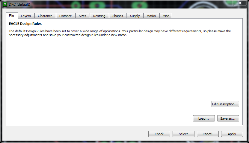
The tabs in this view (Layers, Clearance, Distance, etc.) help define a huge set of design rules which your layout needs to pass. These rules define things like minimum clearance distances, or trace widths, or drill hole sizes…all sorts of fun stuff. Instead of setting each of those manually, you can load up a set of design rules using a DRU file. To do this, hit Load… and select the SparkFun.dru file you just downloaded. The title of the window will change to “DRC (SparkFun)”, and some values on the other tabs will change. Then hit the Check button.
Again, look down to the bottom-left of the editor. If your design is perfect, you should see “DRC: No errors.” But if things didn’t go so swell, you’ll instead be greeted by the dreaded “DRC Errors” window. The error window lists all of the open errors, and it also highlights where the error is. Click on any of the errors listed, and EAGLE will point to the offender.
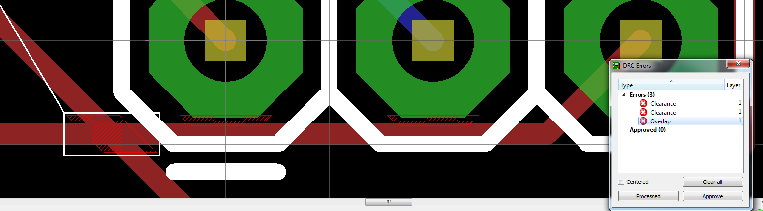
There are all sorts of errors that the DRC can find, but here are some of the most common:
- Clearance: A trace is too close to either another trace or a via. You’ll probably have to nudge the trace around using the MOVE tool.
- Overlap: Two different signal traces are overlapping each other. This will create a short if it’s not fixed. You might have to RIPUP one trace, and try routing it on the other side of the board. Or find a new way for it to reach its destination.
- Dimension: A trace, pad, or via is intersecting with (or too close to) a dimension line. If this isn’t fixed that part of the board will just be cut off.
Once you’ve seen both “No airwires left!” and “DRC: No errors.”, your board is ready to send to the fab house, which means it’s time to generate some gerber files. Before we do that though, let’s add some finishing touches to the design.
Finishing Touches
Adding Copper Pours
Copper pours are usually a great addition to a board. They look professional and they actually have a good reason for existing. Not to mention they make routing much easier. Usually, when you’re adding a copper pour it’s for the ground signal. So let’s add some ground pours to the design.Start by selecting the POLYGON tool –
 . Then (as usual), you’ll need to adjust some settings in the options bar. Select the top copper (1) layer. Also adjust the Isolate setting which defines how much clearance the ground pour gives other signals, 0.012" for this is usually good.
After you’ve drawn the polygon, you have to connect it to a net using the NAME tool –
 .
This works just like naming nets on a schematic. Use that tool on the
dotted red line you just created, and in the dialog that pops up type
“GND”. (Click here to see an animated GIF of the entire process.)
.
This works just like naming nets on a schematic. Use that tool on the
dotted red line you just created, and in the dialog that pops up type
“GND”. (Click here to see an animated GIF of the entire process.)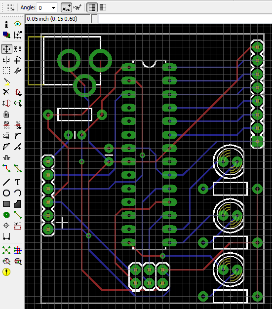
The last step is to hit ratsnest, to watch the glorious red pour fill just about the entire area of your board. You’ll probably hate me for telling you this now, but adding ground pours to your design at the very beginning (after placing parts, before routing) makes manual routing much easier.
You can (and probably should) have ground pours on both sides of the board, so follow the same set of steps on the bottom layer.
It can be hard to tell what is and isn’t connected to the ground pour. If you see a black gap separating a pad and the pour, there is no connection. If you see some traces forming a “target” over the pad, there is a connection from the pour to that pad.
If you ever want to hide the polygon (it’s hard to see other stuff with it on there), use the RIPUP tool on the polygon border you just drew. Don’t worry, the polygon is still there, just hit ratsnest to bring it back.
Adding Silkscreen
Although it has no real effect on the circuit your designing, silkscreen can be a critical part of the PCB design. You want it to look good, right? Some silkscreen – like part outlines – is automatically placed on the board because it’s a piece of the part. We can manually add other information, like labels, logos, and names. A variety of draw tools – wire (), text ( ), circle (
 ), arc (
 ), rectangle (
 ), and polygon () – can be used to draw on the silkscreen layer (tPlace for top, bPlace for bottom).
Have fun and explore with these tools. You could add labels for the headers, or values for the resistors, or even create a nifty logo.
The draw tools are a bit limited, but that doesn’t mean you can’t make it look good!
Generating Gerbers
When you’ve finalized your design, the last step before sending it off to the fab house is to generate gerber files. Gerber files are kind of a “universal language” for PCB designs. EAGLE is far from the only PCB CAD software out there, and its design files are nothing like those of Orcad or Altium. Fab houses can’t possibly support every piece of software out there, so we send them the gerber files instead.Gerber files – note the plurality – each describe single layers of the PCB. One gerber might describe the silkscreen, while another defines where the top copper is. In all, we’ll generate seven gerber files to send to the fab house.
CAM Processor
Before we get too much further, you’ll need to download another definition file: SparkFun’s CAM file.Then, load up the CAM processor by clicking the CAM icon –
 – which will open up this window:
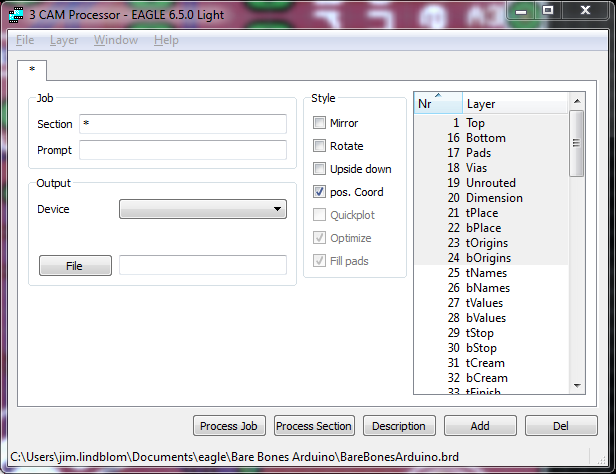
From here, go to the File menu, then go Open > Job…. In the file browser that opens, select the sfe-gerb274x.cam file that you just downloaded. Now the CAM processor window should have a series of tabs: “Top Copper”, “Bottom Copper”, “Top Silkscreen”, etc. Each of these tabs define how to create one of the gerber files. Now all you have to do is click Process Job. If you haven’t saved recently, it’ll prompt you to.
The gerber generation process should be pretty quick. Once it’s run its course, have a look in your project directory, which should have loads of new files in it. In addition to the board (BRD) and schematic (SCH) files, there should now be a .dri, .GBL, .GBO, .GBS, .GML, .gpi, .GTO, .GTP, .GTS, and a .TXT. Meet the Gerbers!
| Gerber File | Extension |
|---|---|
| Bottom Copper | GBL |
| Bottom Silkscreen | GBO |
| Bottom Soldermask | GBS |
| Top Copper | GTL |
| Top Silkscreen | GTO |
| Top Soldermask | GTS |
| Drill File | TXT |
| Drill Station Info File | dri |
| Photoplotter Info File | gpi |
| Mill Layer | GML |
| Top Paste | GTP |
Subscribe to:
Comments (Atom)